XX Workshop on Semiconductors and Micro & Nano Technology
Event integrated with the VI INCT NAMITEC Workshop
SEMINATEC brings together leading researchers, practitioners, and industry experts from around the globe. The Workshop aims to promote the interaction among industry, academy, research & development centers, government, and students, all looking for real opportunities towards improving education, research, and technology.
Seminatec 2026 will be held in conjunction with the VIth Workshop of the INCT NAMITEC network. The program of the two days is common to both events. A special poster session of NAMITEC will be held in parallel to the poster session of Seminatec and a restricted NAMITEC session will be held at the 3rd day, after Seminatec.
Registration deadline for Seminatec 2026 participants: March 31st
All participants, including those not presenting a paper, must complete the registration form. The information provided will be used for event organization and name badge preparation.
Registrations starting from April 1st do not guarantee badges.
Prospective authors must submit their abstract in PDF format.
ABSTRACT PREPARATION
Contributed papers will be selected based on submitted abstracts of up to two pages, two columns in A4 format. Submissions will only be accepted in PDF format and must be submitted before March 2th, 2026.
To download the template, click here. The authors will need to register their email with CMT. Here is a link to how to create a CMT account.
The Microsoft CMT service was used for managing the peer-reviewing process for this conference. This service was provided for free by Microsoft and they bore all expenses, including costs for Azure cloud services as well as for software development and support.
| April 8th, 2026 | April 9th, 2026 | April 10th, 2026 | |||
|---|---|---|---|---|---|
| 08:00 - 09:00 | Registration | 08:00 - 08:30 | Registration | 08:30 - 12:30 | VI Workshop INCT Namitec |
| 09:00 - 09:20 | Opening | 08:30 - 09:00 | IoT and Environmental: "Internet of Natural Things (IoNT): the electronic behind a smart tree" (Prof. Cleonilson Protasio) | 12:30 - 14:00 | Lunch break |
| 09:20 - 10:10 | Distinguished Lecturer 1: "A Review on Dielectric Breakdown in Thin Dielectrics: Silicon Dioxide, High-k, and Layered Dielectrics" (Prof. Felix Palumbo) | 09:00 - 09:50 | Distinguished Lecturer 4: "Evolution from Conventional Planar MOSFETs to Advanced Gate-All-Around (GAA) Nanosheet FETs" (Prof. Adelmo Ortiz) | 14:00 | INCT NanoQuantSS |
| 10:10 - 10:40 | Coffee break | 09:50 - 10:20 | Coffee break | 14:00 - 17:30 | Lab tours (only for NAMITEC attendants) |
| 10:40 - 11:30 | Distinguished Lecturer 2: "Critical Technologies for Chiplet Integration" (Prof. Subramanian S. Iyer) | 10:20 - 10:50 | Photonic Integrated Circuits: "From Photonic Molecules and Integrated Lasers to the Frontiers of Quantum Technology and Neural Network Enablers" (Prof. Newton C. Frateschi) | ||
| 11:30 - 12:10 | Distinguished Lecturer 3: "Cryogenic CMOS for future scaled quantum computing systems" (Prof. Daniel Friedman) | 10:50 - 11:20 | Quantum Technologies: "Spin Qubits em semicondutores: Materiais, Controle e Integração" (Dr. Everton Arrigui) | ||
| 12:10 - 14:00 | Lunch break | 11:20 - 11:50 | Cryo Devices: "Electrical Characteristics of Advanced MOSFETs Operating in Cryogenic Temperatures" (Prof. Marcelo A. Pavanello) | ||
| 14:00 - 14:30 | Brazilian Association of the Semiconductor Industry (ABISEMI) | 11:50 - 13:30 | Lunch break | ||
| 14:30 - 15:00 | Ministry of Science, Technology and Innovation of Brazil (MCTI) | 13:30 - 14:00 | LNNano/CNPEM: "Transistors go Wet: Chemical Sensing and Biosensing by Controlling the Semiconductor/Electrolyte Interface" (Dr. Rafael Furlan) | ||
| 15:00 - 15:40 | INCT NAMITEC | 14:00 - 14:30 | Eldorado Research Institute: Advanced Packaging | ||
| 15:40 - 17:30 | Poster Session I + Coffee | 14:30 - 15:00 | HwIT - Hardware Innovation Technologies: "Converging Photonics and Microelectronics: Building AI Infrastructure" (Dr. Julio Oliveira) | ||
| 17:30 | Closing | 15:00 - 17:00 | Poster Session II + Coffee | ||
| 17:30 | Closing | ||||
DISTINGUISHED LECTURES
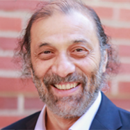
DL 1 – Prof. Felix Palumbo, PhD.
Biography
As a Principal Device Engineer at Allegro MicroSystems, I am a researcher with extensive academic and industrial experience in semiconductor device physics, reliability, and transport phenomena at material interfaces.
I hold a PhD (2005) and MSc (2000) in Physics from the University of Buenos Aires. My contributions include over 100 scientific papers (h-index: 24) with 2,295+ citations, two key review articles, and 6 US patents. My work was recognized with the 2019 IEEE IRPS Best Paper award, and I was an invited speaker in 2015. In recognition of my expertise, I serve as an Editor for the IEEE Transactions on Device and Materials Reliability and as an IEEE-EDS Distinguished Lecturer.
My passion for applied science has led to collaborations with industry leaders like IBM, Tower Jazz, and SOITEC. My international experience includes a Marie Curie EU Fellowship at the Technion–Israel Institute of Technology and visiting researcher roles at institutions in Italy, France, and Spain.
In academia, I am a Full Professor at the National Technological University (UTN) in Buenos Aires, where I have managed over 25 funded research projects and supervised numerous PhD students. My teaching experience spans both undergraduate and graduate levels.
At Allegro, I bridge the gap between device physics and high-volume manufacturing. My responsibilities include defining Design of Experiments (DOE), creating novel test structures, and performing detailed electrical characterization and failure analysis. A key focus is developing and verifying BEOL (Back-End-of-Line) design rules to enhance manufacturing yield and ensure long-term device reliability.
DL talk
“A Review on Dielectric Breakdown in Thin Dielectrics: Silicon Dioxide, High-k, and Layered Dielectrics”
Thin dielectric films are fundamental components in micro- and nanoelectronics, and their reliability has become a critical challenge amidst market demands for ever-improving device performance. The degradation and subsequent breakdown of these films under operational stress are of immense technological importance. This phenomenon is widely investigated in traditional dielectrics (e.g., SiO2, HfO2, Al2O3) and requires thorough investigation in emerging materials, such as layered dielectrics, poised for future device integration.
A comprehensive understanding of both the underlying physical mechanisms and the statistical nature of dielectric breakdown is crucial for ensuring the reliability of modern and future electronic devices. Moreover, a controlled breakdown process offers novel opportunities for fabricating new-concept resistive switching devices, including non-volatile memories and electronic synapses.
This review covers the fundamentals of the dielectric breakdown phenomenon in both traditional and emerging thin dielectrics. We describe the physical triggers for breakdown onset, the resulting structural damage, the statistical modeling of failure, and the broader technological implications, offering perspectives on future challenges and opportunities.
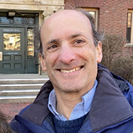
DL 2 – Prof. Subramanian S. Iyer (Subu), PhD.
Biography
Subramanian S. Iyer (Subu) is Distinguished Professor and holds the Charles P. Reames Endowed Chair in the Electrical Engineering Department and a joint appointment in the Materials Science and Engineering Department at the University of California at Los Angeles. In 2023-4, he was on assignment to the US Department of Commerce as Director of the National Advanced Packaging Manufacturing Program, where he laid the foundational strategy for the national packaging imperative. He is the founding Director of the Center for Heterogeneous Integration and Performance Scaling (UCLA CHIPS). Prior to that he was an IBM Fellow. His key technical contributions have been the development of the world’s first SiGe base HBT, Salicide, electrical fuses, embedded DRAM and 45nm technology node used to make the first generation of truly low power portable devices as well as the first commercial interposer and 3D integrated products. Since joining UCLA, he has been exploring new packaging paradigms and device innovations that may enable wafer-scale architectures, in-memory analog compute and medical engineering applications. He is a fellow of IEEE, APS, iMAPS and NAI as well as a Distinguished Lecturer of IEEE EDS and EPS. He is a Distinguished Alumnus of IIT Bombay and received the IEEE Daniel Noble Medal for emerging technologies in 2012 and the 2020 iMAPS Daniel C. Hughes Jr Memorial award and the iMAPS distinguished educator award in 2021.
List of publications/patents:
https://scholar.google.com/citations?user=xXV4oIMAAAAJ&hl=en
DL talk
“Critical Technologies for Chiplet Integration”
Electronics packaging has taken center stage in the evolution of High-performance Computing (HPC) including Artificial Intelligence and Machine Learning (AI/ML) . Packaging performs two functions protecting the chip and serving a system of chips. Advanced packaging is characterized by three vectors: (1) scale-down and scale-out (2) an open chiplet eco-system and (3) a built-in self-test and repair methodology. This has driven a shift from “traditional” packaging where the emphasis has been on the “protection” aspects of single chip packages to one where the “serving” aspects of packaging are emphasized. In this talk, we will discuss the technological underpinnings of advanced packaging especially heterogeneous die-substrate thermal compression bonding (TCB), power delivery and thermal dissipation innovations and most importantly, the test and repair methodology needed to ensure long term reliability. This journey has barely begun and the transition from semiconductor device and chip innovations to electronics packaging innovations will dominate for the next few decades. Furthermore, this transition will rely heavily on innovation made in the semiconductor equipment and integration in the last several decades.
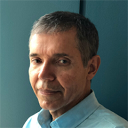
DL 3 – Daniel Friedman, PhD.
Biography
Dr. Daniel Friedman is currently a Distinguished Research Scientist and Senior Manager of the Communication Circuits and Systems department, IBM Thomas J. Watson Research Center, Yorktown Heights, NY, USA; he is also an IEEE Fellow. He received his doctorate from Harvard University and then subsequently completed post-doctoral work at Harvard and consulting work at MIT Lincoln Laboratory. At IBM, he initially developed field-powered RFID tags before turning to high data rate wireline and wireless communication. His current research interests include accelerator designs for AI, high-speed I/O design, phase-locked-loop design, millimeter-wave circuits and systems, and circuit/system approaches to enabling new computing paradigms, the latter including cryogenic electronics for use in quantum computing systems. He holds more than 90 patents and has authored or coauthored more than 85 publications. He was a co-recipient of the Beatrice Winner Award for Editorial Excellence at the 2009 International Solid-State Circuits Conference (ISSCC), the 2009 Journal of Solid-State Circuits (JSSC) Best Paper Award (given in 2011), the 2017 ISSCC Lewis Winner Outstanding Paper Award, and the 2017 JSSC Best Paper Award (given in 2019). He has served on the technical program committees of the Bipolar Circuits and Technology Meeting (2003-2008) and of the ISSCC (2008-2016); since 2016, he has served as the ISSCC Short Course chair. He served as a member-at-large of the IEEE Solid-State Circuits Society (SSCS) Adcom from 2018-20, as the SSCS Distinguished Lecture chair from 2020 to 2021, and as Associate Editor of the JSSC from 2019-2023. He is the current Vice President of the SSCS.
DL talk
“Cryogenic CMOS for future scaled quantum computing systems.”
Quantum computing represents a new paradigm that has the potential to transform problems that are computationally intractable today into solvable problems in the future. Significant advances in the last decade have lent support to the idea that quantum computers can be implemented, and further that the goal of demonstrating true performance advantages over traditional computing techniques on one or more problems may be achieved in the not so distant future. Delivering on this promise is expected to require quantum error correction solutions, in turn demanding large qubit counts that pose significant challenges for quantum computer implementations, especially in the area of qubit interface electronics. An active area of research to address this challenge is the use of integrated cryogenic CMOS designs. In this presentation, we will present a superconducting qubit-based quantum computing system framework, opportunities for cryogenic CMOS introduction into future systems, example cryogenic CMOS implementations and results, and next challenges that must be met to enable cryogenic CMOS adoption.
DL 4 – Prof. Adelmo Ortiz-Conde, PhD.
Biography
Adelmo Ortiz-Conde received the professional Electronics Engineer degree from Universidad Simón Bolívar (USB), Caracas, Venezuela, in 1979 and the M.E. and Ph.D. from the University of Florida, Gainesville, in 1982 and 1985, respectively.
From 1979 to 1980, he served as an instructor in the Electronics Department at USB. In 1985, he joined the technical Staff of Bell Laboratories, Reading, PA, where he was engaged in the development of high voltage integrated circuits. In 1987, he returned to the Electronics Department at USB where he was promoted to Full Professor in 1995. He was on sabbatical leave at University of Central Florida (UCF), Orlando, from January to August 1994, and again from July to December 1998. He also was on sabbatical leave at “Centro de Investigaciones y Estudios Avanzados” (CINVESTAV) National Polytechnic Institute (IPN), Mexico City, Mexico, from October 2000 to February 2001.
He has coauthored one textbook, Analysis and Design of MOSFETs: Modeling, Simulation and Parameter Extraction (2012 Springer reprint of the original 1st ed. 1998, http://dx.doi.org/10.1007/978-1-4615-5415-8 ), over 200 international technical journal and conference articles (including 22 invited review articles). His present research interests include the modeling and parameter extraction of semiconductor devices.
Dr. Ortiz-Conde is an EDS Distinguished Lecturer and the Vice-Chair of IEEE’s CAS/ED Venezuelan Chapter. He was editor of IEEE Electron Device Letters in the area of Silicon Devices and Technology from 2009 to 2018. He was the Region 9 Editor of IEEE EDS Newsletter from 2000 to 2005. He is a Member of the Editorial Advisory Board of various technical journals: Microelectronics and Reliability, “Universidad Ciencia y Tecnología” and “Revista Ingeniería UC”. He regularly serves as reviewer of several international journals and conferences. He was one of the founders of the first IEEE International Caracas Conference on Devices, Circuits, and Systems (ICCDCS) in 1995. In order to make it more international, this conference changed its name to “International Caribbean Conference on Devices, Circuits, and Systems (ICCDCS)” in its sixth edition in 2006. Since 2019, this conference has been sponsored by the IEEE Electron Devices Society (EDS) under the name of “IEEE Latin America Electron Devices Conference (LAEDC)”.
DL talk
“Evolution from Conventional Planar MOSFETs to Advanced Gate-All-Around (GAA) Nanosheet FETs “
We review the origins, evolution and present status of MOSFETs, which has been the dominant semiconductor device in electronics applications for more than 4 decades. The conceptual invention of MOSFET, by Lilienfeld in 1928, and the end of World War II, in 1945, inspired Bell Labs to research into semiconductors. Bardeen and Brattain, who were working in the Semiconductor Sub-Group at Bell Labs, fabricated the first point contact transistor in December,1947. This achievement motivated Shockley, who was the group leader, to invent the bipolar junction transistor in January 1948. Bardeen, Brattain and Shockley received the Nobel Prize in 1956 “for their discovery of the transistor effect.” After solving oxide reliability problems, the MOSFET was fabricated in 1960 by Kahng and Atalla. The invention of CMOS, by Wanlass and Sah in 1963, made the MOSFET to be the most commonly used device in digital applications. The transistors have been miniaturized for more than fifty years, following Moore’s Law from 1965, and they are now approaching their final limits in the nanometer regime. Recent innovations, such as strained silicon and high-k metal gates are being used in modern MOSFETs. The classical planar MOSFETs were replaced with 3D FinFETs in 2012, and with gate-all-around (GAA) Nanosheet FETs in 2025. The GAA nanosheet FETs used in the industry are composed of nanosheets stacked vertically, with the current flowing horizontally. In research labs, new vertical GAA FETs are being developed; these are composed of nanosheets stacked horizontally, with the current flowing vertically.
GUEST SPEAKERS
Prof. Cleonilson Protasio, PhD
UFPB
Prof. Newton Frateschi, PhD
UNICAMP
Prof. Marcelo Pavanello, PhD
FEI
Prof. Everton Arrighi, PhD
Brazilian Nanotechnology National Laboratory (LNNano)
Prof. Rafael Furlan, PhD
Brazilian Nanotechnology National Laboratory (LNNano)
Prof. Julio Oliveira, PhD
HwIT – Hardware Innovation Technologies
Auditório Milton Santos
Instituto de Geociências (IG) – UNICAMP
Rua Carlos Gomes, 250
CEP: 13083-855 – Campinas, SP
General Chair: Marcos Puydinger – FEEC/UNICAMP
Program Chair: Marco Roberto Cavallari – FEEC/UNICAMP
Program Committee
Local Organizing Committee